Intel Foundry resurfaces: It will manufacture Google TPUs and courts NVIDIA
Intel secures a key contract to manufacture 3nm artificial intelligence chips for Google and positions itself as an alternative to TSMC with its 18A technology.
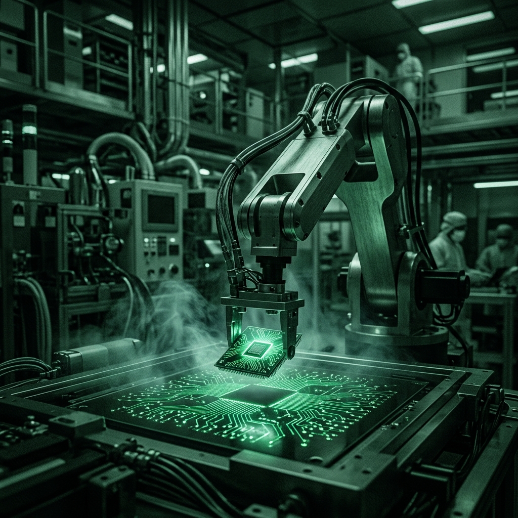
Intel Foundry resurfaces: It will manufacture Google TPUs and courts NVIDIA
In the volatile and crucial semiconductor manufacturing market, Intel has scored a vitally important strategic goal. Its independent manufacturing division, Intel Foundry, has secured a multi-million dollar contract to produce Google's next generation of tensor processing units (TPUs) using its advanced 3 nanometer node.
This milestone represents a boost of confidence for the American firm after years of performance problems and financial restructuring, positioning it as the strongest Western alternative to the monopoly of the Taiwanese TSMC.
Google's diversification and courtship of NVIDIA
Google has been developing its own AI acceleration chips (TPUs) for years to power its cloud computing ecosystem and power models like Gemini. Historically, the company relied on TSMC to manufacture these complex designs. By shifting part of its volume to Intel, Google not only ensures a more diverse supply chain, but helps establish a manufacturing competitor on North American and European soil.
But the most striking movement on Intel's horizon is the rapprochement with NVIDIA. NVIDIA officials have confirmed that they are evaluating test wafers from Intel's 18A (1.8 nm class) manufacturing process.
Currently, NVIDIA is almost completely tied to TSMC for the manufacturing of its sought-after GPUs for AI data centers. With the constant risk of a geopolitical conflict in the Taiwan Strait that would cripple the global economy, NVIDIA urgently needs a secure, geographically distributed manufacturing option.
Cadena de Suministro de Chips de IA (Transición 2026)
┌─────────────────────────────────┐      ┌─────────────────────────────────┐
│   Histórico (TSMC Taiwán)       │      │   Futuro Diversificado          │
│   • Google TPUs: TSMC           │  =>  │   • Google TPUs: Intel 3nm      │
│   • NVIDIA GPUs: TSMC           │      │   • NVIDIA GPUs: TSMC + Intel   │
└─────────────────────────────────┘      └─────────────────────────────────┘
##The value of process 18A
Intel's 18A node is CEO Pat Gelsinger's big bet to regain technological leadership in transistor density and efficiency. It introduces two key innovations to silicon architecture:
- RibbonFET Transistors: A total redesign of the transistor structure that improves current flow and reduces energy leakage.
- PowerVia: The first implementation of power delivery through the back side of the silicon wafer. This allows the data lines to be separated from the power supply lines, eliminating interference and enabling higher processing frequencies with lower thermal consumption.
If Intel can demonstrate that it can mass produce 18A wafers at stable yield rates, it could wrest a substantial share of the world's most profitable AI hardware contracts from TSMC, redefining the geopolitics of semiconductors in favor of the West.
Frequently Asked Questions (FAQ)
What agreement have Intel and Google reached for AI chips?
Intel will manufacture a strategic batch of AI accelerators (TPUs) for Google using its advanced manufacturing technologies at the 3-nanometer node.
Why is NVIDIA considering using Intel manufacturing technology?
NVIDIA seeks to diversify its manufacturing suppliers to reduce dependence on TSMC (Taiwan) in the face of growing geopolitical tensions and capacity shortages.
How relevant is Intel's 18A manufacturing process?
The 18A process (equivalent to 1.8nm) represents Intel's technological spearhead, which promises to surpass competing nodes through new transistor technologies and rear-side power delivery.